Abstract

This site provides detailed constructional information for the realisation of three 8 bit bidirectional parallel ports in a GameBoyTM cartridge. Only limited hardware knowledge is required, but elementary laboratory equipment is expected. To rebuild the shown cartridges a manufacturing capability for PCBs is required with an programming capability for EPROM or Flash. The job should be done in about less than 15h.
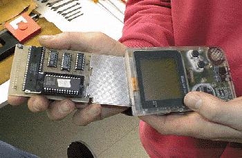
the ready etched board
Figure 0: the ready etched board

Ver 1.0


0.0 Introduction
0.1 The Game Boy - only a rusty game console ?
0.2 Who are we ?
1.0 What is inside the Game Boy ?
1.1 Technical detail
1.2 Address overview
1.3 Memory mapping
1.4 Cartridge types
2.0 The project idea
2.1 What is missing in the GB-hardware ?
3.0 Building the hardware
3.1 How to connect an Eprom
3.1.1 The GB-Adapter
3.2 The 8255 a PI/O - Chip
3.3 How to get the right hardware address
3.4 The GB-I/O interface board
4.0 Building the software
4.1 Software development tools
4.2 First steps using GB-Basic
4.3 The program
5.0 Future development
Appendix A: downloads
A.1 The GB-Adapter board
A.2 The GB-PIO board
A.3 Other Downloads
Appendix B: Miscellaneous stuff
B.1 PI/O 82C55 FAQ
B.2 Useful documents
B.3 ISA Flash card

With special thanks to Jeff Frohwein and all members
of the "GameBoy development ring"


People Resources This GameBoy Development Ring site
is owned by Marc Rawer
[ Skip Prev ] [ Prev ] [ Next ] [ Skip Next ]
[ Random ] [ Next 5 ] [ List Sites ] [ Site Stats ]

Game Boy & Nintendo are trademarks
of Nintendo Co., Ltd. of Kyoto, Japan.

This document was created with StarOffice 4.0 by Marc Rawer