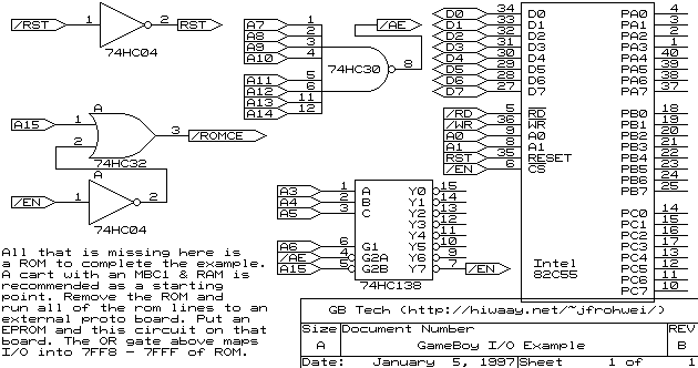
This section describes how to combine to combine the 82C55A with an EPROM so that the three ports of the 8255 will be mapped from 7FF8h to 7FFAh and the mode register to 7FFFh. This requires logic to provide address decoding for each device.. This can be easily realized with the circuit shown in Figure 13 .
Figure 13: Wiring diagram for the device switching logic
Description:
The 74HC30 and the 74HC138 are
used as NANDs to decode the state whereby all the address lines
A3..A14 are high and A15 is low. This will result in a low at /EN (Y7
of 74HC138). This state occurs when the GameBoyTM is
accessing the address area 7FF8h to 7FFFh /EN can be wired to /CS of
the 8255 and when low will activate the RD/WR-control logic of the
8255.
The
ROM on the other side requires the inverted impulse (EN). This is
generated by an inverter in the 74HC04. This signal is then ORed with
A15 to make sure that the EPROM is off when the GameBoyTM
accesses an address over 7FFFh. The last step is inverting /Rst of
the GameBoyTM
to provide a reset for the 8255.
In principal the GB-I/O interface board is functionally the same as the circuit diagram shown in figure 13. We just realized the logic in full-NOR-technology to reduce the IC count in doing this we eliminated the 74HC04 and the 74HC32 and put in a 74HC04.
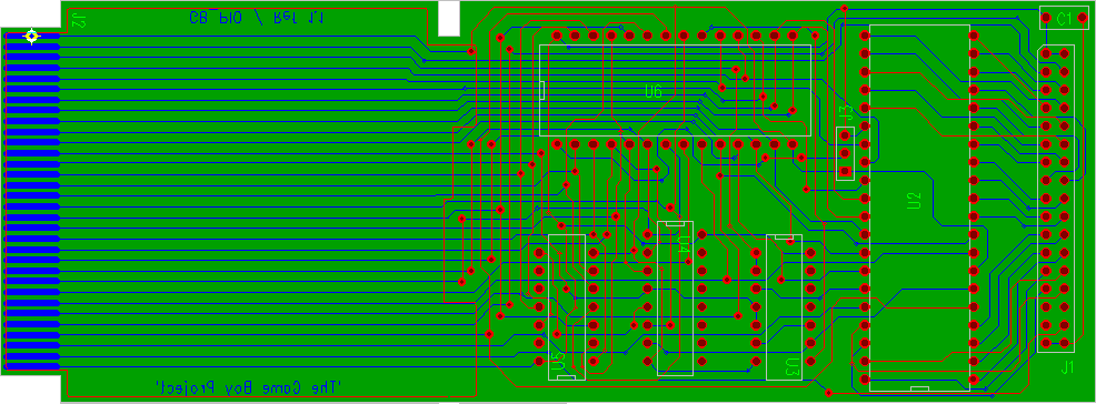
Figure 14: GB-I/O interface board layout
|
U2 |
Intel 82C55A (DIP) |
J1 |
Header 34 pin (2.54mm grid) |
|---|---|---|---|
|
U3 |
74HC00 (DIP) |
J3 |
Jumper |
|
U4 |
74HC138 (DIP) |
C1 |
Capacitor (100nF) |
|
U5 |
74HC30 (DIP) |
Cx |
5 * Capacitor for each IC between Vcc/Gnd |
|
U6 |
NM27C512Q120 (DIP) (='EPROM 64k+8) |
board |
double sided 100 mm * 160 mm |
 Figure
14 displays the board layout. To download
the ready to etch layout plans simply click on the image.
Note that the board is viewed from the component side through the
board to the solder side.
Figure
14 displays the board layout. To download
the ready to etch layout plans simply click on the image.
Note that the board is viewed from the component side through the
board to the solder side.
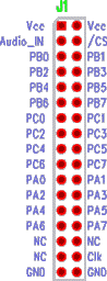
Figure 15 shows the pinout of the
34pin header J1 of the GB PI/O interface board. The purpose of the
header is to allow expansion for further devices. Vcc, ground, clock,
U3 chip select and the three ports are available on the header.